Loading the model
This device cannot show the 3D model. You can read the guide steps below as text.
1 / 8 A transistor cut in half This is an n-channel MOSFET, cut through the middle and drawn hundreds of thousands of times larger than life. Two blue islands of n-type silicon, the source and the drain, sit in a p-type substrate. With 0 V on the gate and 2 V on the drain, the meter reads zero.
Drag to turn. Scroll or pinch to zoom.
Guide Parts Controls
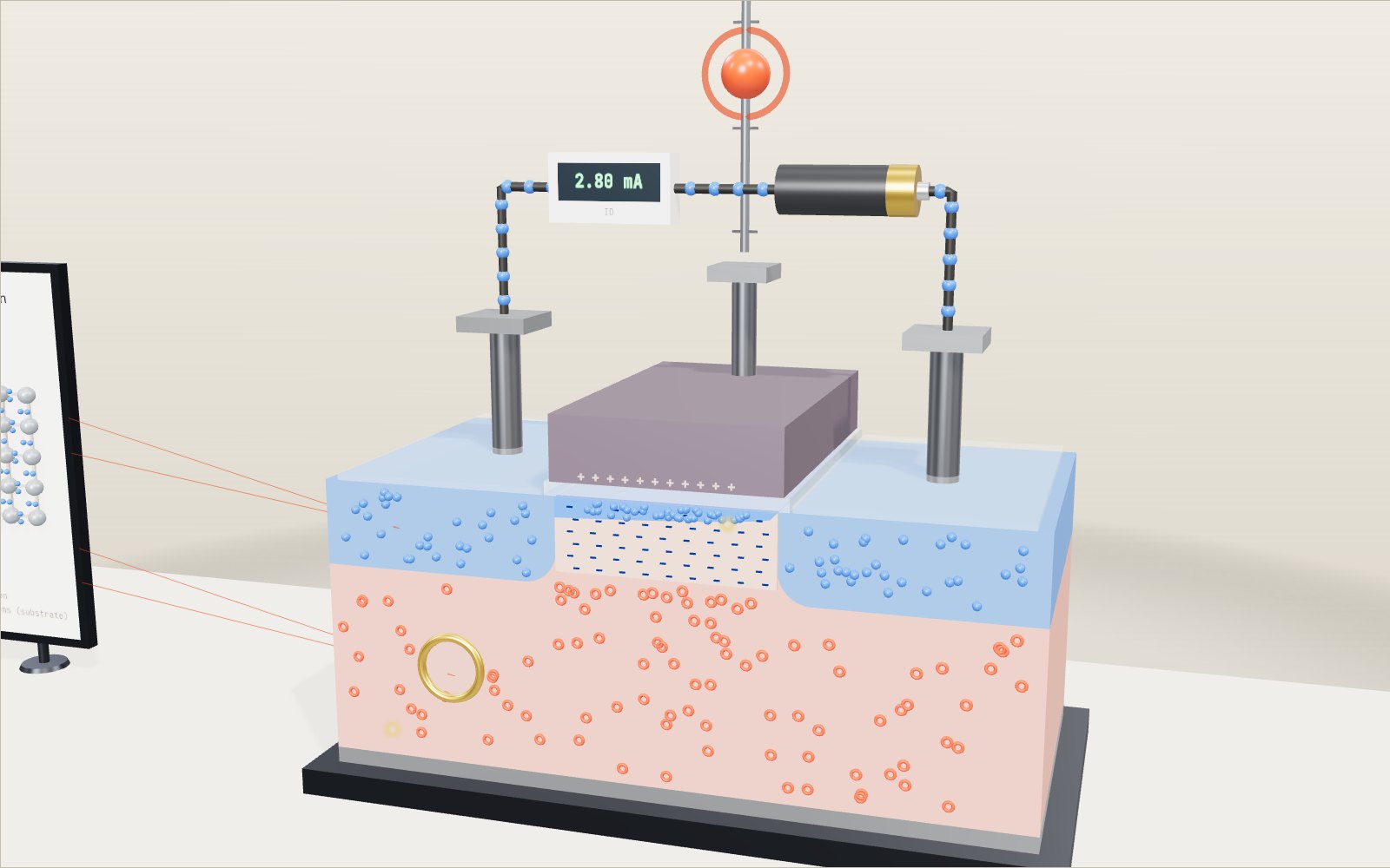
01 A transistor cut in half This is an n-channel MOSFET, cut through the middle and drawn hundreds of thousands of times larger than life. Two blue islands of n-type silicon, the source and the drain, sit in a p-type substrate. With 0 V on the gate and 2 V on the drain, the meter reads zero.
02 Silicon with a few foreign atoms Pure silicon conducts poorly because every outer electron is held in a bond. Put a phosphorus atom in and its fifth electron wanders free, which makes n-type silicon. Boron has only three, so one bond is short of an electron. That gap, the hole, hops from bond to bond.
03 The gate pushes the holes away At 0.5 V the gate carries a little positive charge. It cannot touch the silicon, since 10 nm of oxide lies in between, but its field reaches through and drives the holes down. Left behind near the surface are fixed negative boron ions: a depletion region.
04 Past the threshold a channel appears Above the 0.7 V threshold, the field draws enough electrons to the surface to turn it n-type. This thin inversion layer joins source to drain. At 1.2 V about 72,000 electrons sit in the channel and the meter shows 0.22 mA.
05 More gate, much more current In the square-law model the current grows with the square of the voltage above threshold. At 2.5 V it reaches 2.8 mA. The drain is at only 2 V, so the channel thins toward the drain and pinches off at its end, and raising the drain voltage now changes little.
06 Two transistors make a switch The board on the right puts a p-channel transistor over an n-channel one. With 3.3 V in, the nMOS conducts and pulls the output to 0 V, so the LED goes dark. Move the inverter input slider down and the pMOS takes over. At either end one transistor is off, so almost no current flows.
07 A small wiggle becomes a big one The gate now swings 50 mV either side of 1.2 V. The current follows at 0.86 mA per volt of gate swing. Sent through a 10 kΩ resistor, that current change moves the output 8.6 times as far as the input moved. This is amplification.
08 From one to sixteen billion The chip in front stands for Apple's M1, which Apple says holds 16 billion transistors; counting one a second would take 507 years. Beside it is a replica of the first transistor, the point-contact device Bardeen and Brattain got working at Bell Labs in December 1947.
p-type substrate The silicon body, doped with boron at about 10¹⁷ atoms per cm³, one for every 500,000 silicon atoms. Its free charges are holes (red rings). Source (n+) An island doped heavily with phosphorus, about one atom in 500. It is full of free electrons (blue dots) and supplies the electrons that cross the channel. Drain (n+) The same kind of island as the source. With a positive voltage on it, electrons that arrive through the channel leave by the drain contact. Gate oxide Silicon dioxide, 10 nm thick in the model. It insulates the gate, so the gate works on the silicon through its electric field alone and draws no steady current. Gate The control electrode on top of the oxide. Its voltage decides whether a channel exists. The pale plus signs show its positive charge. Inversion layer (channel) A thin sheet of electrons drawn to the surface once the gate passes the 0.7 V threshold. Its thickness follows the square-law charge profile, so it thins toward the drain. Depletion region The layer under the gate with its holes pushed away, leaving fixed negative boron ions (dark blue dashes). It deepens up to the threshold and then stops growing. Contacts and outside circuit Tungsten plugs and aluminium pads join source and drain to a supply and a current meter. The gate has its own plug at the back, with the red knob. Doped silicon lattice Silicon atoms share electrons in pairs. Phosphorus (P) brings one electron too many, boron (B) one too few, and the missing one is a hole. CMOS inverter A p-channel transistor above an n-channel one, gates tied together. The output is the opposite of the input. The small screen plots output against input. Chip package A processor die on its package. Apple's M1 holds 16 billion transistors. Intel's 4004 of 1971 held 2,300. Point-contact transistor, 1947 A replica of the Bell Labs device: two closely spaced gold contacts held by a plastic wedge, pressed onto a small slab of germanium.