FIG. 72How It Works
How a transistor works as a switch: the MOSFET gate
A chip with 16 billion transistors turns each one on and off with a few volts on a gate that never touches the silicon underneath.
This device cannot show the 3D model. You can read the guide steps below as text.
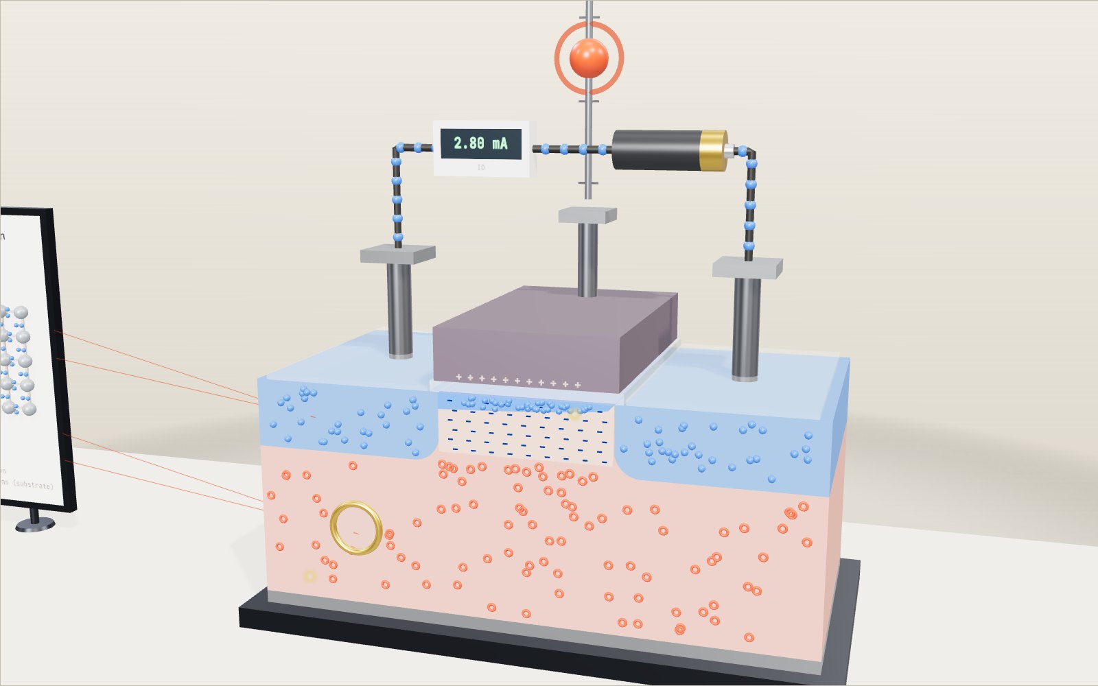
1 / 8 A transistor cut in halfThis is an n-channel MOSFET, cut through the middle and drawn hundreds of thousands of times larger than life. Two blue islands of n-type silicon, the source and the drain, sit in a p-type substrate. With 0 V on the gate and 2 V on the drain, the meter reads zero.
Drag to turn. Scroll or pinch to zoom.
What the model shows
A MOSFET transistor switches on when gate voltage draws enough electrons beneath the oxide to form a conducting channel. That channel joins the source and drain so current can flow. The insulated gate controls the channel without needing a steady current through the oxide.
A phone or laptop processor is a slab of silicon with billions of switches on it, and none of them has a moving part. Each one turns a current on and off because a voltage on one electrode changes what the silicon underneath is made of, at least for the few nanometres nearest the surface. This exhibit shows how that works in the most common kind of transistor, the n-channel MOSFET (metal-oxide-semiconductor field-effect transistor).
The block in the middle is one transistor cut down the middle, so you are looking at its cross-section. The blue islands are the source and the drain, the pink body is the substrate, the thin pale layer on top is the gate oxide and the block above it is the gate. Plugs and pads connect the source and drain to a supply and a current meter, and the gate has its own plug at the back. The cut face shows the charges: red rings are holes, blue dots are free electrons, and dark blue dashes are boron ions that cannot move. On the left a panel shows the silicon lattice with one foreign atom in each half. On the right a small board pairs two transistors into an inverter, the simplest logic gate. In front sit a chip package and a replica of the first transistor of 1947.
The gate voltage slider is the main control. The readout plots drain current against gate voltage, and the dot shows where the transistor is on that curve.
Silicon that barely conducts
Each silicon atom has four outer electrons and shares them with four neighbours, two electrons to each bond. In a perfect crystal at room temperature almost every one of those electrons is held in place. Only about 10¹⁰ per cubic centimetre are shaken free by heat, out of 5 × 10²² atoms, so pure silicon is a poor conductor.
Doping changes that. Replace one silicon atom with phosphorus, which has five outer electrons, and four go into bonds while the fifth is held so loosely that it wanders off at room temperature. Silicon with extra electrons like this is n-type. Boron has only three outer electrons, so one of its four bonds is an electron short. A neighbouring electron can hop into that gap, which moves the gap one bond over. The moving gap behaves like a positive charge and is called a hole. Silicon with extra holes is p-type.
It takes very little. The model's substrate has 10¹⁷ boron atoms per cubic centimetre, one for every 500,000 silicon atoms. The source and drain are doped far harder, with 10²⁰ phosphorus atoms per cubic centimetre, one in 500.
Why no current flows at first
With the gate at 0 V, follow the path an electron would have to take from source to drain. It leaves an n-type island full of electrons, crosses p-type silicon full of holes, and enters the other n-type island. Each boundary between n and p is a pn junction, and the two face opposite ways. However you connect the supply, one of them is reverse biased and blocks the current. That is why the meter reads zero even with 2 V on the drain.
To get current across, the strip of p-type silicon between the islands has to become n-type. The gate does exactly that, and it does it without touching the silicon.
How the gate reaches through the oxide
The gate sits on a layer of silicon dioxide, 10 nanometres thick in the model. The oxide is an insulator, so the gate, the oxide and the silicon form a capacitor. Put a positive voltage on the gate and positive charge collects on it. An equal negative charge has to gather on the other side of the oxide, in the silicon.
At first the silicon finds that negative charge by giving up holes. Set the gate to 0.5 V and watch: the holes under the gate are pushed down, leaving the boron ions behind. Each boron ion took an electron into its bonds when its hole left, so it carries a fixed negative charge. The emptied layer is the depletion region. It deepens as the gate voltage rises, up to the threshold.
The threshold and the inversion layer
Above a certain gate voltage, pushing holes away no longer supplies the charge, and electrons start to collect at the surface instead. They come in from the source next door, which is full of them. Once there are more electrons than holes in that thin surface layer, the layer has turned n-type. It is called the inversion layer, and it is the channel: a continuous n-type path from source to drain.
The gate voltage at which this happens is the threshold voltage, set at 0.7 V in the model. In a real process it depends on the substrate doping, the oxide thickness and the gate material, and manufacturers tune it with an extra implant of dopant. Past the threshold the depletion region stops growing, and every extra volt on the gate goes into more electrons in the channel.
Checking the square law with numbers
The simplest useful model of a MOSFET is the square law, and the exhibit uses it directly. Start with the oxide. Its capacitance per unit area is
Cox = εox / tox = (3.9 × 8.854 × 10⁻¹² F/m) / (10 × 10⁻⁹ m) = 3.45 × 10⁻³ F/m², or 0.345 µF/cm².
Each volt above the threshold, called the overdrive, puts Cox × 1 V of electron charge under every square centimetre of gate. At 1.2 V on the gate the overdrive is 0.5 V, which works out to 1.08 × 10¹² electrons per square centimetre.
How fast those electrons move depends on their mobility, taken as 500 cm²/V·s in the channel. Multiply mobility by Cox and you get the process constant k′ = 173 µA/V². The channel is 10 µm wide and 1 µm long, so β = k′ × W/L = 1.73 mA/V².
When the drain voltage is large enough, the drain current is
Id = ½ β (Vgs − Vt)².
At 1.2 V that gives ½ × 1.73 mA/V² × (0.5 V)² = 0.216 mA. At 2.5 V the overdrive is 1.8 V and the current is 2.80 mA, and at 3.3 V it is 5.84 mA. Doubling the overdrive from 0.5 V to 1.0 V multiplies the current by four, which is why the curve in the readout bends upward. Below 0.7 V the model gives exactly zero.
You can also count the electrons. With the drain at 2 V and the gate at 1.2 V, the channel holds about 72,000 of them, and dividing their charge by the current gives the time one electron takes to cross: about 53 picoseconds. At 2.0 V on the gate it falls to 20 picoseconds.
Why the channel pinches off at the drain end
The electrons in the channel feel the gate voltage relative to the silicon beneath them, and that silicon is at 0 V near the source but at the drain voltage near the drain. So the overdrive shrinks along the channel, and so does the electron sheet. In the model the channel is drawn with that profile, thick at the source and thinning toward the drain.
When the drain voltage is small, the channel behaves like a resistor and the current rises in step with the drain voltage. This is the linear region. With 3.3 V on the gate and 0.1 V on the drain the current is 0.44 mA, a resistance of about 227 Ω. That is the state a transistor is in when it is used as a closed switch.
Raise the drain voltage until it equals the overdrive and the electron sheet thins to nothing at the drain end. This is pinch-off. Electrons still cross, swept through the short high-field gap by the drain, but more drain voltage barely adds to the current. The transistor is in saturation. In step 5, with 2.5 V on the gate, the current is 2.24 mA with 1 V on the drain and 2.80 mA at both 2 V and 3.3 V.
Two transistors make an inverter
A logic gate needs a transistor that pulls the output down and another that pulls it up. CMOS (complementary MOS) uses an n-channel transistor for the first job and a p-channel one for the second. The p-channel device is the mirror image: p-type source and drain in an n-type well, switched on when its gate is well below its source.
On the board both gates are tied to the input. With 3.3 V in, the nMOS is on and the pMOS is off, so the output is pulled to 0 V and the LED is dark. With 0 V in it is the other way round and the output sits at 3.3 V. At either end one transistor is off, so there is no path from supply to ground and the circuit draws almost nothing while it holds its state. Current flows only during switching.
In the model the pMOS is made 2.5 times wider to make up for holes moving more slowly than electrons. That puts the switching point at 1.65 V, half the supply, where 0.84 mA flows briefly through both transistors. Combine gates like this one and you can build the circuit in How logic gates add numbers.
How a transistor amplifies
The same curve that makes a good switch also makes an amplifier. Hold the gate at 1.2 V, in saturation, and let it wiggle 50 mV either way. The slope of the curve there, the transconductance gm = β (Vgs − Vt), is 0.86 mA per volt, so the current moves by about 43 µA each way.
Feed the drain from a 5 V supply through a 10 kΩ resistor and that current change becomes a voltage change across the resistor. The drain sits at 2.84 V and swings between 2.39 V and 3.25 V, a swing of 0.86 V for 0.1 V in. The voltage gain is gm × R = 8.6. The output also moves the opposite way to the input, so this circuit is called an inverting amplifier. Turn on the small signal control to see the input and output swings marked on the curve.
Sixteen billion on one chip
Apple says its M1 chip of 2020 holds 16 billion transistors. If you counted one every second without stopping, you would finish after 507 years. Apple's M3 Max of 2023 holds 92 billion, and NVIDIA says its Blackwell-architecture GPUs hold 208 billion. For comparison, the Intel 4004 microprocessor of 1971 had 2,300, so the M1 has about seven million times as many.
They fit because modern transistors are tiny, with gates tens of nanometres long instead of the model's 1 µm, and gates that wrap around the channel on several sides instead of sitting on top. The principle is the one shown in the block: a gate voltage that creates or removes a conducting channel.
What the model leaves out
- Short channels. The square law holds for long channels like the model's 1 µm. In short ones the electrons reach a top speed, and the current grows more nearly in proportion to the overdrive than to its square.
- Current below threshold. Real transistors leak a small current below the threshold, falling by a factor of ten for each 60 mV or more of gate voltage at room temperature. The model sets it to zero.
- Channel-length modulation. In saturation the current still creeps up slowly with drain voltage. The main model leaves this out. The inverter adds a small slope of 0.05 per volt so its output has one value at every input.
- Scale. The charges are drawn far larger and far fewer than real ones, and the oxide is drawn thicker relative to the channel.
- Shape. The gate and the islands run straight back into the block. Modern chips use fin and gate-all-around shapes.
From a germanium slab to the MOSFET
The idea of controlling a current with a field came first. Julius Lilienfeld filed a patent for a field-effect device in 1926, but attempts to build one through the 1930s did not succeed. At Bell Labs, William Shockley conceived a field-effect amplifier in 1945 that did not work as intended. John Bardeen suggested that electrons at the semiconductor surface were blocking the field, and he and Walter Brattain set out to study those surface states.
On 16 December 1947 they got the first semiconductor amplifier working. Two closely spaced gold contacts, held in place by a plastic wedge, pressed on a small slab of high-purity germanium. A voltage on one contact controlled the current through the other and amplified a signal up to 100 times. They showed it to Bell Labs officials on 23 December, the engineer John Pierce gave it the name transistor, and Bell Labs announced it at a press conference on 30 June 1948. Shockley, Bardeen and Brattain shared the 1956 Nobel Prize in Physics.
The surface problem was solved with oxide. In 1959 M. M. (John) Atalla and Dawon Kahng at Bell Labs made the first working insulated-gate field-effect transistor on thermally grown silicon dioxide. In 1963 C. T. Sah and Frank Wanlass of Fairchild showed that pairing p- and n-channel transistors drew close to zero power in standby, and Wanlass patented the idea now called CMOS.
The energy needed to change a bit
An insulated gate does not need a continuous conduction current in the ideal model, but it still needs charge. The gate and channel form a capacitor, and the wiring and the gates of the next circuit add more capacitance. To change a voltage, a driver must move that charge. MIT's computation structures course describes this relation as Q = CV. A useful distinction is between keeping a bit unchanged and changing it repeatedly: the second activity can consume considerable power even when the first needs very little.
For a numerical example, assume a total switched capacitance of 1 fF and a voltage swing of 1 V. These are assumed values for a calculation, not measurements of the exhibit or specifications of a particular processor. The charge needed is 1 fC. The energy stored at the end of charging is ½CV² = 0.5 fJ. With ordinary resistive charging from a fixed voltage supply, the supply delivers CV² = 1 fJ: half becomes stored energy and half becomes heat during charging. Discharging then dissipates the stored half. A complete charge-and-discharge cycle therefore dissipates 1 fJ in this simplified circuit, not 0.5 fJ. Energy-recovery circuits can work differently; they are not represented here.
Suppose that node completes 1 billion such cycles each second. Its average switching power is 1 µW. If 1 million identical nodes did that together, their combined switching power would be 1 W. This example does not mean that every transistor in a billion-transistor chip switches on every clock tick. Many nodes hold their value, and different blocks run at different times. A clock frequency counts timing cycles, not the number of transitions made by every transistor. The activity factor in P = αCV²f expresses how often a node actually charges from low to high per timing cycle.
Now reduce the assumed voltage from 1 V to 0.8 V without changing capacitance or activity. The switching energy becomes 0.64 of its previous value, a reduction of 36 percent. The square matters. But a lower voltage also reduces transistor drive current and can make a logic path slower or unreliable. The power saving is therefore constrained by the time allowed for signals to settle. This is why a processor's voltage and frequency settings are linked rather than independent knobs that can be moved without consequences.
Leakage and the limit of the off state
The flat zero-current part of the exhibit's curve is a modelling choice. A real MOSFET has subthreshold current even when its gate voltage is below the nominal threshold. Carriers can cross a potential barrier through thermal motion. The barrier changes continuously with gate voltage, so the physical device does not abruptly jump from perfect insulation to conduction at exactly 0.7 V. The threshold is a useful engineering reference, not a mechanical latch clicking shut.
Other leakage paths include reverse-biased junctions and current through an extremely thin gate insulator. Their relative importance depends on the device technology, dimensions, temperature and operating voltage. Modern gate stacks use materials and thicknesses chosen to retain electrostatic control while limiting leakage. A gate that wraps farther around the channel helps suppress unwanted source-to-drain conduction, but does not eliminate every path by which charge can escape.
A second assumed calculation shows why small currents matter in large chips. At 1 V, a leakage current of 1 nA corresponds to 1 nW. If 1 billion devices each leaked that much under the same conditions, the total would be 1 W even without useful switching. Real chips do not have identical leakage in every device: transistor types, logic states and temperature vary. The calculation is a scale illustration rather than a prediction for the M1. It explains why disconnecting the supply to an idle block, called power gating, can save more energy than merely stopping its clock. Clock gating reduces switching activity; it does not by itself remove leakage.
What transistor counts and process names mean
The Computer History Museum traces Moore's observation to a 1965 article. His original extrapolation was a doubling of components per integrated circuit each year; in 1975 he revised the longer-term rate toward a doubling about every two years. It was an observation and an industry target, not a physical law requiring every processor to double its count on a fixed anniversary. It also concerned economical integration, not a promise that every program would run twice as fast.
Compare the historical 2,300-transistor Intel 4004 with the 16 billion transistors Apple reports for M1. Dividing the second count by the first gives about 7 million. That ratio is about component count, not a performance benchmark. M1 contains caches, graphics and other functional blocks as well as processor cores, and the two chips have very different architectures, word sizes and workloads. A substantial fraction of a modern chip's transistors can be used to store bits rather than perform arithmetic. Comparing only the headline count hides those differences.
A process name such as a nanometre node should not be read as the measured length of every gate on the chip. Roadmaps such as IEEE IRDS distinguish physical quantities including gate length and pitches between repeating structures. A pitch measures the repeat spacing of features; it is not the same thing as the length of a conducting channel. Different manufacturers' node names are not a shared ruler. To make a meaningful comparison, specify the quantity, the measurement method and the circuit being compared rather than equating a marketing label with one physical dimension.
The shape changes as well. In a planar MOSFET the gate lies above a flat channel. In a FinFET, a narrow fin rises from the surface and the gate controls several sides. In a gate-all-around device, the gate surrounds a narrow channel, often arranged as stacked sheets or wires. Bringing the gate around the channel improves its control relative to the drain's electric field, which becomes increasingly troublesome as devices get shorter. These are different geometries of field control, not tiny mechanical contacts opening and closing. The exhibit keeps a planar section so the inversion layer and fixed dopant ions remain easy to see; it is not a geometrical drawing of a current manufacturing node.
Experiments with the existing controls
Use “Gate voltage” with “Drain voltage” kept at 2 V. First set the gate below 0.7 V, then move it above the threshold. The model changes from no conducting channel to an inversion layer. Near threshold, compare two settings whose overdrives differ by a factor of 2 while both remain in saturation. The ideal square law predicts a current ratio of 4. Compare the readout rather than counting the animated electrons: their number and speed have been chosen to make charge motion visible, not to reproduce every carrier in the physical device.
Next keep the gate above threshold and reduce “Drain voltage” to zero. A channel can exist while the net drain current vanishes because there is no drain-to-source voltage driving it. Raise the drain voltage gradually and compare the low-voltage resistive region with saturation. Saturation does not mean the channel is empty or current has stopped. It means that raising drain voltage no longer increases current strongly in the ideal long-channel model. Do not confuse this MOSFET use of “saturation” with the terminology used for a bipolar transistor switch.
Finally move “Inverter input” across its range and observe the output, then enable “Small signal on gate” for the amplifier illustration. The inverter maps a range of inputs to opposite logic levels; the amplifier uses a chosen operating point and small changes around it. Neither the moving markers nor the small-signal animation is a measurement of a processor's maximum clock speed. The exhibit contains no GHz timing experiment, gate-capacitance meter or temperature control. The energy and leakage calculations above are paper experiments that extend the visible model, not hidden controls to search for on the screen.
From one switch to a computer: the five scenes
The buttons along the top of the stage move through five scenes, each a step further out. The first is the cut-open MOSFET. A red knob sits on a rail above the gate: grab it and drag it up, and the gate voltage rises with it. Past 0.7 V the channel appears and the meter starts to read. A gold ring on the cut face is a magnifier. Drag it over the substrate, the source, the depletion layer or the channel, and a panel shows what a cube 10 nm on a side would hold at that spot in this model: about 50,000 silicon atoms everywhere, about 100 phosphorus atoms and as many free electrons in the n+ islands, but only 0.1 boron atom on average in the substrate. The channel row counts electrons in a 10 nm square of the inversion layer instead, because the layer is a sheet only a few nanometres thick. At 2.5 V on the gate that is about 4 electrons at the source end, fewer towards the drain. These are model values worked out from the doping and the oxide capacitance used throughout this page, not measurements of a particular chip.
The second scene puts two circuit boards side by side, the third holds a half adder, the fourth zooms out from a single transistor to a whole chip and down again to atoms, and the fifth compares three transistor shapes. Numbers on the stage that come from the model rather than from a published source carry an asterisk.
Two transistors make NOT, four make NAND
The right board is the CMOS inverter described above: one pMOS above one nMOS, their gates tied together. The left board is a NAND gate built from four transistors. Two pMOS sit side by side between the 3.3 V rail and the output, so either of them can pull the output up. Two nMOS sit one above the other between the output and ground, so both must be on to pull it down. The output is therefore 0 only when input A and input B are both 1. In every other case at least one pMOS is on and at least one nMOS is off, so the output sits at 3.3 V.
Press A and B, or tap the white switches on the board, and the traces change colour: warm for 1, blue for 0. The channel strip of each transistor lights when it conducts. The truth table in the panel marks every input pair you have tried. In steady state no current flows from the supply to ground in either board, because for each input pair one side of the gate is always off. CMOS draws current mainly while it switches, which is why billions of these gates can sit on one chip without melting it.
The jumper between the boards connects the NAND output to the inverter input. NAND followed by NOT gives AND: the LED on the inverter board lights only for 1 and 1. NAND is said to be functionally complete, meaning any logic function can be built from NAND gates alone, and the next scene uses nothing else.
Five NAND gates add two bits
A half adder takes two one-bit numbers and gives a sum bit S and a carry bit C. The adder on the board uses five NAND gates. The first, N1, takes A and B. N2 and N3 each combine one input with the output of N1, and N4 combines N2 and N3: that output is A XOR B, the sum bit. N5 has both inputs tied to N1, which turns it into an inverter, so its output is A AND B, the carry. With four transistors per CMOS NAND gate, the whole adder holds 20 transistors.
Try the four pairs. 0 + 0 = 00, 0 + 1 = 01, 1 + 0 = 01 and 1 + 1 = 10 in binary: the carry is the "tens" digit of base two. A full adder, which also accepts a carry from the column to its right, is the building block of every multi-digit adder. The logic adder exhibit chains such stages to add whole numbers. For scale, the Intel 4004 of 1971, the first commercial microprocessor, had 2,300 transistors in total.
Zooming out: from 1947 to a few nanometres
The fourth scene is a zoom bar that covers more than seven powers of ten. At the widest view the screen is about 6 cm across and shows a chip package with its die and, beside it, the replica of the 1947 point-contact transistor. The die is drawn as a model chip 11 mm square with 16 billion transistors, the count Apple gives for its M1. The replica base is drawn about 15 mm wide (model value). The first transistor and a modern chip are, in other words, about the same size, and one held 1 transistor while the other holds 16 billion.
Zoom in and the layers change: one processor core, then rows of standard logic cells, then transistors standing side by side, then a single nanosheet transistor about 60 nm across, and finally the silicon atoms of one sheet, 0.235 nm apart. Things of the same size appear at the same scale along the way: a human hair 80 µm thick, a red blood cell 7.5 µm across, a transistor of the Intel 4004 with its 10 µm features, and a virus 100 nm across (the hair, cell and virus sizes are typical model values). The readout shows the width of the screen and how many transistors fall inside it at the model density of about 132 per square micrometre. A view about 2.75 mm wide already holds a billion of them.
The nanosheet at the bottom is drawn 5 nm thick, inside the range the IEEE International Roadmap for Devices and Systems gives for current devices. Silicon atoms sit 0.235 nm apart, so the sheet is only about 21 atoms thick. At that size a few stray atoms or a single missing layer change how the transistor behaves, which is one reason the shapes in the next scene matter.
Why transistors grew fins and then sheets
The fifth scene shows three transistors cut through the middle of the gate, with current flowing towards you. In the planar transistor the gate sits on top of a flat channel and controls it from one face. In the FinFET the channel stands up as a thin fin and the gate wraps three faces. In the gate-all-around (GAA) nanosheet transistor the channel is a stack of thin sheets and the gate surrounds each one on all four faces.
The difference shows when the gate gets short. A transistor is never perfectly off: some electrons still cross the channel, and the drain's electric field reaches under the gate and lowers the barrier they must climb. A useful measure is the subthreshold swing, the gate voltage needed to change the off current tenfold. At room temperature it can never be smaller than about 60 mV per decade (kT/q times ln 10). The weaker the gate's grip on the channel, the larger the swing and the more current leaks when the transistor should be off. That leakage flows all the time in every idle transistor on the chip, so it becomes heat.
The stage uses a simple model with a "natural length" λ for each shape, 8, 4 and 3 nm (model values): swing = 60 mV per decade × (1 + 3 e^(−L/2λ)), and drain-induced barrier lowering = 0.15 V × e^(−L/2λ). Drag the gate length from 100 nm down to 8 nm. At 100 nm all three shapes reach almost the ideal swing. At 20 nm the planar transistor's on/off ratio has fallen to about 1,600, while the FinFET still keeps about 150,000 and the GAA transistor close to a million. At 8 nm only the GAA shape keeps the off current more than 1,000 times below the on current in this model. The numbers are illustrative; real devices depend on doping, oxide, strain and many other choices.
The history follows the same line. Intel's 45 nm process of 2007 replaced the silicon dioxide gate insulator, which had become thin enough to leak, with a hafnium-based high-k insulator and a metal gate. Its 22 nm process of 2011 introduced the Tri-Gate, or FinFET, transistor. Samsung started production of 3 nm chips with GAA nanosheet transistors in June 2022, and TSMC's first nanosheet process, N2, entered volume production in the fourth quarter of 2025.
Moore's law with real chips
In 1965 Gordon Moore observed that the number of components on a chip was doubling every year, and in 1975 he revised the rate to every two years. The chart under the stage plots chips by year against the transistor count their makers published, on a scale that rises ten times per line: from the Intel 4004 (1971, 2,300 transistors) through the 8086 (1978, 29,000), the Intel386 (1985, 275,000) and the Pentium 4 (2000, 42 million) to Apple's M1 (2020, 16 billion), NVIDIA's Blackwell data-centre processor (2024, 208 billion) and Cerebras' wafer-sized WSE-3 (2024, 4 trillion). The dashed line doubles every two years from the 4004. Tap a dot to read the chip, the year and the source.
Below the chart you can pick the chip in your own phone or computer, or type its count, and compare it with the world's population, about 8.2 billion people in 2024 according to the United Nations. An Apple M1 holds about 2 transistors for every person on Earth. Counting its 16 billion transistors one per second, without a break, would take about 507 years.
Questions
What does a transistor actually do?
It lets a small signal control a larger current. In a MOSFET the voltage on the gate decides whether a conducting channel exists between source and drain and how many electrons are in it. Used fully on or fully off, it is a switch. Used partway, it is an amplifier.
What is the threshold voltage of a MOSFET?
It is the gate voltage at which enough electrons collect under the gate to form a channel. Below it the transistor is off. The exhibit uses 0.7 V, a common textbook figure. Real values depend on doping, oxide thickness and gate material.
Why does the gate not draw current?
The gate is separated from the silicon by a layer of oxide, which is an insulator. Charge flows onto the gate only while its voltage changes, as with any capacitor, and then stops. That is a large part of why CMOS chips use so little power while idle.
What is the difference between n-type and p-type silicon?
N-type silicon has a few atoms with five outer electrons, such as phosphorus, mixed in, giving it spare electrons. P-type has atoms with three, such as boron, which leave holes. In the model the substrate has one boron atom per 500,000 silicon atoms.
What is the difference between the linear and saturation regions?
In the linear region the drain voltage is small and the channel behaves like a resistor. In saturation the drain voltage is larger than the overdrive, the channel pinches off at the drain end and the current depends mainly on the gate voltage.
How many transistors are on a chip?
It varies widely. Apple says its M1 has 16 billion and its M3 Max 92 billion. NVIDIA says its Blackwell GPUs have 208 billion. The Intel 4004 of 1971, an early single-chip processor, had 2,300.
Who invented the transistor?
John Bardeen and Walter Brattain made the first working transistor, a germanium point-contact device, at Bell Labs in December 1947. They shared the 1956 Nobel Prize in Physics with William Shockley, who led the group. The first working MOSFET came from Atalla and Kahng at Bell Labs in 1959.
Why do computers use CMOS?
In a CMOS gate one transistor of each pair is always off when the input is steady, so almost no current flows from supply to ground. Power is used mainly while switching, which lets billions of transistors run from a phone battery.
Does a 1 GHz clock mean every transistor switches a billion times a second?
No. It describes timing cycles. Individual nodes may retain their values, and disabled blocks may not switch at all. Switching power depends on capacitance, voltage and actual activity as well as frequency.
Is half CV squared the energy of a whole switching cycle?
It is the energy stored on a charged capacitor. Ordinary resistive charging and discharging dissipates CV² over a complete cycle. Confusing stored energy with the energy supplied during a cycle underestimates this loss.
Does a smaller process name give the exact gate length?
No. A node name identifies a technology generation, not one universal physical dimension. Gate length, fin or sheet geometry and structure pitches must be examined separately.
Terms
- MOSFET: metal-oxide-semiconductor field-effect transistor, in which a gate on an insulating oxide controls a channel in the silicon.
- Source and drain: the two heavily doped regions the channel connects. In an n-channel device electrons enter at the source and leave at the drain.
- Gate oxide: the thin insulating layer between gate and channel.
- Doping: adding a small amount of another element to silicon to give it spare electrons (n-type) or holes (p-type).
- Hole: a missing electron in a bond, which moves through the crystal like a positive charge.
- Depletion region: a layer from which the mobile charges have been pushed out, leaving fixed ions.
- Inversion layer: a thin layer at the surface where the gate has turned p-type silicon n-type. It forms the channel.
- Threshold voltage (Vt): the gate voltage at which the channel forms.
- Overdrive: the gate voltage above threshold, Vgs − Vt.
- Pinch-off: the point where the channel thins to nothing at the drain end, the start of saturation.
- Transconductance (gm): how much the drain current changes per volt of gate voltage.
- CMOS: complementary MOS, logic built from pairs of n-channel and p-channel transistors.
Sources
Computer History Museum, The Silicon Engine: 1947, Invention of the Point-Contact Transistor. https://www.computerhistory.org/siliconengine/invention-of-the-point-contact-transistor/ (checked 17 October 2026)
Computer History Museum, The Silicon Engine: 1926, Field Effect Semiconductor Device Concepts Patented. https://www.computerhistory.org/siliconengine/field-effect-semiconductor-device-concepts-patented/ (checked 17 October 2026)
Computer History Museum, The Silicon Engine: 1960, Metal Oxide Semiconductor (MOS) Transistor Demonstrated. https://www.computerhistory.org/siliconengine/metal-oxide-semiconductor-mos-transistor-demonstrated/ (checked 17 October 2026)
Computer History Museum, The Silicon Engine: 1963, Complementary MOS Circuit Configuration is Invented. https://www.computerhistory.org/siliconengine/complementary-mos-circuit-configuration-is-invented/ (checked 17 October 2026)
Computer History Museum, The Silicon Engine: 1971, Microprocessor Integrates CPU Function onto a Single Chip. https://www.computerhistory.org/siliconengine/microprocessor-integrates-cpu-function-onto-a-single-chip/ (checked 17 October 2026)
Nobel Prize Outreach, The Nobel Prize in Physics 1956. https://www.nobelprize.org/prizes/physics/1956/summary/ (checked 17 October 2026)
Apple Newsroom, Apple unleashes M1 (10 November 2020). https://www.apple.com/newsroom/2020/11/apple-unleashes-m1/ (checked 17 October 2026)
Apple Newsroom, Apple unveils M3, M3 Pro, and M3 Max (30 October 2023). https://www.apple.com/newsroom/2023/10/apple-unveils-m3-m3-pro-and-m3-max-the-most-advanced-chips-for-a-personal-computer/ (checked 17 October 2026)
NVIDIA, NVIDIA Blackwell Architecture. https://www.nvidia.com/en-us/data-center/technologies/blackwell-architecture/ (checked 17 October 2026)
PVEducation (C. Honsberg and S. Bowden), Doping. https://www.pveducation.org/pvcdrom/pn-junctions/doping (checked 17 October 2026)
PVEducation, General Properties of Silicon (atomic density, intrinsic carrier concentration). https://www.pveducation.org/pvcdrom/materials/general-properties-of-silicon (checked 17 October 2026)
MIT OpenCourseWare, 6.012 Microelectronic Devices and Circuits, Fall 2009: Lecture Notes (MOSFET square-law model, CMOS inverter). https://ocw.mit.edu/courses/6-012-microelectronic-devices-and-circuits-fall-2009/pages/lecture-notes/ (checked 17 October 2026)
Model values (oxide capacitance, β, drain currents, electron counts, transit times, amplifier gain, inverter switching point and the counting time for 16 billion) were worked through by hand.
MIT OpenCourseWare, Computation Structures: Sequential Logic (capacitors and Q = CV). https://ocw.mit.edu/courses/6-004-computation-structures-spring-2017/pages/c5/c5s1/ (checked 23 October 2026)
Computer History Museum, 1965: Moore’s Law Predicts the Future of Integrated Circuits. https://www.computerhistory.org/siliconengine/moores-law-predicts-the-future-of-integrated-circuits/ (checked 23 October 2026)
IEEE IRDS, Roadmap editions (device and system scaling). https://irds.ieee.org/editions/2023 (checked 23 October 2026)
Intel, Intel Chips timeline (transistor counts and process sizes from the 4004 to the third-generation Core). https://www.intel.com/content/dam/www/public/us/en/documents/corporate-information/history-intel-chips-timeline-poster.pdf (checked 27 October 2026)
Intel, Intel Reinvents Transistors Using New 3-D Structure (4 May 2011). https://www.intc.com/news-events/press-releases/detail/655/intel-reinvents-transistors-using-new-3-d-structure (checked 27 October 2026)
K. Mistry et al., A 45nm Logic Technology with High-k+Metal Gate Transistors, Strained Silicon, 9 Cu Interconnect Layers, 193nm Dry Patterning, and 100% Pb-free Packaging, IEEE IEDM 2007. https://doi.org/10.1109/IEDM.2007.4418914 (checked 27 October 2026)
Samsung Newsroom, Samsung Begins Chip Production Using 3nm Process Technology With GAA Architecture (30 June 2022). https://news.samsung.com/global/samsung-begins-chip-production-using-3nm-process-technology-with-gaa-architecture (checked 27 October 2026)
TSMC, 2nm Technology. https://www.tsmc.com/english/dedicatedFoundry/technology/logic/l_2nm (checked 27 October 2026)
Apple Newsroom, Apple unveils all-new iPad Air with A14 Bionic (15 September 2020); Apple unveils M1 Ultra (8 March 2022); Apple introduces M4 chip (7 May 2024). https://www.apple.com/newsroom/2022/03/apple-unveils-m1-ultra-the-worlds-most-powerful-chip-for-a-personal-computer/ (checked 27 October 2026)
IEEE Spectrum, Cerebras WSE-3: Third Generation Superchip for AI (13 March 2024). https://spectrum.ieee.org/cerebras-chip-cs3 (checked 27 October 2026)
United Nations, UN projects world population to peak within this century (World Population Prospects 2024). https://www.un.org/en/UN-projects-world-population-to-peak-within-this-century (checked 27 October 2026)
Computer History Museum, The Silicon Engine: 1959, Practical Monolithic Integrated Circuit Concept Patented. https://www.computerhistory.org/siliconengine/practical-monolithic-integrated-circuit-concept-patented/ (checked 27 October 2026)
MIT OpenCourseWare, 6.004 Computation Structures (CMOS gates, NAND as a universal gate, adders). https://ocw.mit.edu/courses/6-004-computation-structures-spring-2017/ (checked 27 October 2026)
Model values added in the five scenes (10 nm cube counts, die size and density, replica size, natural lengths λ and the leakage formula) were worked through by hand.
More exhibits

How a touchscreen works: how the glass finds your finger
Under the glass of a phone lies a grid of transparent electrodes, and your finger shows up as a small dip in the charge passing between them.
How logic gates add numbers: sum bits and carry bits
Adding 7 and 9 on this board takes 20 gates, and the last carry lands 8 gate delays after you flip the switches.
Electric motor simulator: how it works, step by step
Eight motors, from Faraday's wire in mercury in 1821 to the magnets inside an electric car, all turning on the same push between current and field.
How lightning and thunder work
A lightning channel heats the air to about five times the temperature of the Sun’s surface, and its thunder needs about 3 seconds to cover each kilometre to you.
How electricity gets to your home
Electricity leaves the power station at 345,000 volts and reaches the outlet at 220, because high voltage keeps the current, and the heat lost in the wires, small.
How a microwave oven works: the magnetron that makes the waves
The waves inside a microwave oven are 12.2 cm long, so without a turntable the hot spots in your food sit about 6 cm apart.